UNIST site map
- Admissions
-
Academics
- Colleges and Schools
-
Academic Affairs
- Academic Calendar
- Academic Curriculum
- Requirements for Graduation
- Browse Open Courses
- Undergraduate Administration
-
Graduate Academic Affairs
- Tuition Fee Payment
- Academic Leave of Absence/ Academic Return
- Voluntary Withdrawal/ Expulsion
- Change of Major
- Change of Degree Program/ Dropping of Degree Program
- Class Period/ Attendance Period/ Academic Year・Semester
- Course Registration
- Course Drop
- Attendance/ Grade/ Exam
- Credit Transfer/ Credit Carryover
- Academic Forms
- Education Support
-
Research/Industry
- Research Aims
- Research Findings
- Researcher Search
-
Research Organizations
- UNIST Multi-Interdisciplinary Institute
- IBS Research Groups
-
UNIST Labs
- Department of Mechanical Engineering
- School of Energy and Chemical Engineering
- Department of Civil
- Department of Materials Science and Engineering
- Department of Nuclear Engineering
- Department of Industrial Engineering
- Department of Design
- Department of Biomedical Engineering
- Department of Biological Sciences
- Department of Electrical Engineering
- Department of Computer Science and Engineering
- Department of Mathematical Sciences
- Department of Chemistry
- Department of Physics
- School of Business Administration
- Graduate School of Carbon Neutrality
- Graduate School of Artificial Intelligence
- Research Support
- University-Industry Relations
- Campus Life
- News Center
- About UNIST
-
etc
- UNIST Bulletin
- Work-Life Balance Support System
- UNIST Gender Equality Plan
- Faculty Invitation for Tenure Track
- Faculty Invitation for Non-Tenure Track
- Board Meeting Minutes
- University Council Meeting Minutes
- Administrative Service Charter
- Privacy Policy
- Copyright Policy
- Rejection of Unauthorized Email Collection
- Operation and Management Policy for Video Information Processing Devices
- Information Disclosure


Connection Points of Knowledge, Everything About UNIST
Try searching.
Recommended search terms


- portal
- U Academics Innovation Center
- Leadership Center
- Dormitory
- Academic Information Center
- International Students Support
- Browse Open Courses
- Course Registration
- Graduation Requirements for Graduation
- Academic Leave of Absence/ Academic Return
- Military Service
- Certificate Issuance
- Academic Calendar
- Scholarships
- Campus Map
- Campus Life Guidebook
- Health Care Center
- Human Rights Center
- portal
- Job Opening
- Announcement for Bid
- UNIST AI Services
- UNIST Daycare Center
- Sports Center
- UI Downloads
- Announcement
- Recruitment of Professors (Non-tenure)
- Faculty Invitation for Tenure Track
- UNIST Academic Information Center
- Office of Research Facilities and Training
- Office of Research Affairs
- Rule Management System
- Academic Calendar
![]()
![]()
This is a collection of menus necessary for UNIST students .
students
- portal
- U Academics Innovation Center
- Leadership Center
- Dormitory
- Academic Information Center
- International Students Support
- Browse Open Courses
- Course Registration
- Graduation Requirements for Graduation
- Academic Leave of Absence/ Academic Return
- Military Service
- Certificate Issuance
- Academic Calendar
- Scholarships
- Campus Map
- Campus Life Guidebook
- Health Care Center
- Human Rights Center
![]()
![]()
This is a collection of menus necessary for prospective UNIST Students .
prospective Students
![]()
![]()
This is a collection of menus necessary for UNIST Faculty & Staff .
Faculty & Staff
- portal
- Job Opening
- Announcement for Bid
- UNIST AI Services
- UNIST Daycare Center
- Sports Center
- UI Downloads
- Announcement
- Recruitment of Professors (Non-tenure)
- Faculty Invitation for Tenure Track
- UNIST Academic Information Center
- Office of Research Facilities and Training
- Office of Research Affairs
- Rule Management System
- Academic Calendar


NEWS CENTER
Discover not only Research Findings and event news, but also the diverse facets of UNIST presented by reporters and writers.
News Center

UNIST News
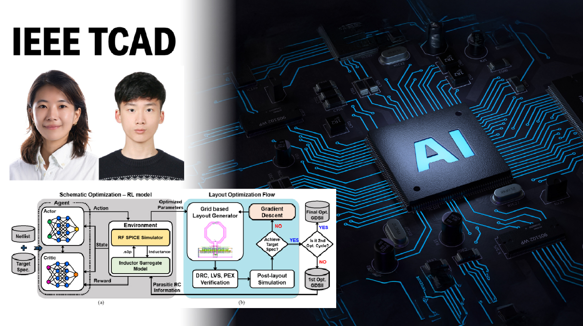
Revolutionizing Semiconductor Design: AI Cuts Development Time from Months to Just One Day
UNIST and KNU researchers develop automated AI solution for high-performance communication circuits.
- Research
- JooHyeon Heo
- 2026.05.12
- 30
Abstract
A team of researchers from UNIST and Kyungpook National University (KNU) has unveiled a pioneering AI system capable of completing the complex design of high-performance semiconductor circuits in just one day—an achievement that drastically reduces the traditional development timeline, which can take several months.
Led by Professor Heein Yoon of UNIST’s Department of Electrical Engineering and Professor Taigon Song of KNU, the team developed an integrated AI platform that automates the entire process—from schematic design to physical chip layout. This breakthrough technology streamlines a typically multi-stage, resource-intensive task, offering faster, more efficient, and highly optimized circuit design solutions.
The initial focus was on the design of the Inductor-Capacitor Voltage-Controlled Oscillator (LC-VCO), a critical component in 5G and emerging 6G communication systems. LC-VCOs generate the carrier signals essential for high-speed data transmission. Designing these circuits involves balancing numerous variables—such as inductor and transistor sizes—to minimize noise and power consumption. However, translating schematic designs into physical layouts often introduces parasitic effects that can impair performance.
The new model integrates circuit schematic optimization with physical layout design, addressing these challenges holistically. During the schematic phase, reinforcement learning algorithms explore various parameter configurations to meet specific frequency and performance targets. Subsequently, in the layout phase, the system employs gradient descent methods to iteratively refine physical design parameters—such as wire widths and spacing—to enhance overall circuit performance. Gradient descent, a well-established optimization technique, incrementally adjusts design variables by following the gradient of the objective function toward an optimal solution.
This integrated approach drastically accelerates the design process. Tasks that previously required up to 119 hours can now be completed in approximately 28.5 hours—reducing the overall time by over 76%. Moreover, the system’s adaptability across different semiconductor process nodes is enabled by transfer learning. Models trained on one technology node (e.g., 65nm) can be efficiently adapted to others (such as 40nm or 28nm), using just around 10% additional data.
This AI-driven methodology not only shortens development cycles and reduces costs but also addresses the industry’s growing need for efficient design automation amid a global talent shortage. By ensuring high performance while minimizing manual effort, this technology is poised to significantly impact the production of next-generation communication and AI chips. The researchers anticipate expanding this framework beyond LC-VCOs to automate various analog and RF circuit designs, further accelerating innovation in semiconductor technology.
The research was led by Sungjin Kim of UNIST and Hyunsoo Lee of KNU, who served as co-first authors, with additional contributions from Hong Seong-min of KNU.
The findings of this research have been published online in the IEEE Transactions on Computer-Aided Design of Integrated Circuits and Systems (TCAD) on April 3, 2026. The study has been supported by the Ministry of Science and ICT (MSIT), the National Research Foundation of Korea (NRF), the Ministry of Education (BK21 Four), the Ministry of Trade, Industry and Energy (MOTIE), the Semiconductor Design Education Center (IDEC), Samsung Electronics, Axion Co., Ltd., and the Institute for Information & Communications Technology Planning & Evaluation (IITP).
Journal Reference
Sungjin Kim, Hyunsoo Lee, Seongmin Hong, et al., "A Framework of Automated LC-VCO Design with Physical Layout Based on Reinforcement Learning, IEEE TCAD, (2026).
Related Links


-
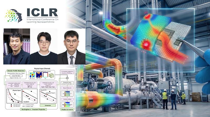
New AI Algorithm to Enhance Accuracy of Thermal and Stress Predictions in Semiconductors
-
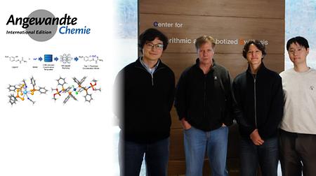
When Chemical Intuition Meets Neural Networks: Hybrid AI Algorithm Predicts Metal–Ligand Coordination Structures
-
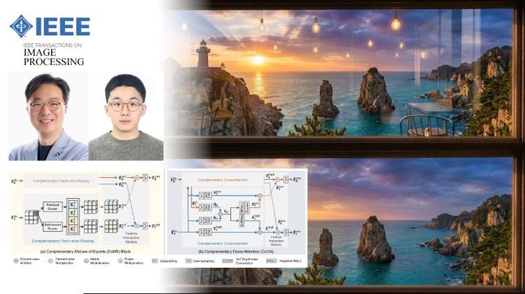
New Study Unveils Adaptive AI Breakthrough for Reflection Separation in the Wild
-
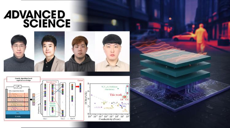
AI-Optimized Vanadium Oxide Multilayers for More Than 20-fold Enhancement in Bolometric Performance