UNISTUNIST

ADMISSIONS

발전기금
모바일메뉴 열기
 

UNIST site map

전체 메뉴 닫기
STUDENT
 
Scroll Down

UNIST Today

we are all

pioneers!

UNIque & beST

Nexus

UNIST Today

we are all

pioneers!

UNIque & beST

Nexus

Information for UNISTar

WHY UNIST

star

Global
Campus for
Future
Innovators

Research AREA

중점연구분야

Research
AREA

에너지·AI·미래산업에 집중하다

UNIST는 에너지 전환, AI, 미래산업이라는
대한민국의 핵심 과제에 연구 역량을 집중합니다.

  • 에너지 전환
  • 이차전지 · 수소 · 탄소중립
  • Ai 기반 산업 혁신
  • 반도체 · 소재 · 양자
EDUCATION INNOVATION

교육혁신프로그램

EDUCATION
INNOVATION

이론을 배우는 것을 넘어 직접
연구하며 성장하다

UNIST의 학부생부터 대학원생까지 연구의
보조가 아닌 주체로 성장하는 경험을 제공합니다.

  • 학부생 연구참여
  • 국제학회·논문참여
  • 소수정예 밀착 연구지도
industry collaboration

산학협력

industry
collaboration

연구에서 산업까지, 현장과 가장
가까운 UNIST

대한민국 최대 산업도시 울산에 위치한
UNIST는 연구 성과가 기업과 산업 현장으로
가장 빠르게 연결되는 구조를 갖추고 있습니다.

  • 기술사업화·창업지원
  • 울산 산업단지
  • 대기업 · 공기업과의 공동연구
Research support

연구지원

Research
support

젊은 UNIST, 연구에 최적화된
유연한 캠퍼스

UNIST는 가장 늦게 출범한 과기원으로,
관행에 얽매이지 않는 유연한 연구·교육 시스템을
갖추고 있습니다.

  • 빠른 신흥 분야 대흥
  • 단일 캠퍼스 기반
  • 생활.연구 일체형 구조
  • 개방형 연구 공간

Research Impact

star

수개월 걸리던 반도체 설계, AI가 ‘단 하루’ 만에 끝낸다!

반도체 설계 전문가가 수주에서 수개월씩 걸려 작업하던 고성능 통신 반도체 회로 설계를 단 하루 만에 끝낼 수 있는 인공지능 기술이 개발됐다. UNIST 전기전자공학과 윤희인 교수와 경북대학교 송대건 교수팀은 통신 회로인 LC 전압제어 발진기(LC-VCO)를 회로 설계 단계부터 실제 칩에 넣는 물리적 레이아웃까지 자동으로 설계해주는 AI 모델을 개발했다고 5일 밝혔다. LC-VCO는 5G 같은 고속 통신 시스템에서 주파수를 만들어내는 반도체 회로다. 신호 잡음과 전력 소모를 줄이기 위해서는 인덕터, 트랜지스터 크기와 같은 변수를 잘 조합해 회로를 설계해야 하는데, 설계된 회로를 실제 칩 안으로 옮기기 위한 레이아웃 설계 단계에서는 회로 설계 단계의 조합이 깨지기 쉽다. 배선 굵기와 소자 배치에 따라 기생 효과가 더해지면서 주파수와 잡음 특성이 다시 달라질 수 있기 때문이다. 연구팀이 개발한 모델은 회로 설계와 레이아웃 설계를 통합해 최적화할 수 있다. 회로 설계 단계에서는 강화학습을 적용해 설계 변수들을 바꿔가며 목표 주파수와 성능을 만족하는 조합을 찾도록 했고, 실제 칩 구조가 결정되는 레이아웃 단계에서는 경사하강법을 이용해 배선 폭과 간격 같은 물리적 설계 변수를 성능이 개선되는 방향으로 반복적으로 보정하는 방식이다. 경사하강법은 현재 상태에서 성능이 더 좋아지는 방향을 따라 설계 값을 조금씩 조정해 최적의 조건을 찾아가는 최적화 기법이다. 연구팀은 “회로도 설계(Schematic)와 물리적 배치(Layout)를 개별적으로 최적화하던 기존 방식을 대신 AI가 두 단계를 통합적으로 관리하도록 한 기술”이라고 설명했다. 설계 과정에서 가장 시간이 오래 걸리는 인덕터는 딥러닝 기반 예측을 활용해 전체 설계 시간을 크게 줄였다. 설계자의 반복적인 전자기 시뮬레이션이 필요하던 작업을 단 몇 밀리초(ms) 만에 완료된다. 실험 결과, 기존의 자동 설계 방식이 약 119시간 소요되던 작업을 단 28.5시간 만에 완료해 설계 시간을 76% 이상 단축했다. 성능 지수(FoM) 또한 기존 연구 대비 월등히 우수한 결과를 보였다. 또 전이 학습이 적용돼 반도체 나노 공정 노드가 바뀌어도 기존에 학습한 내용을 바탕으로 설계를 이어갈 수 있다. 예를 들어 65nm 공정으로 학습한 AI는 40nm나 28nm 공정에서도 처음 학습에 필요했던 데이터의 약 10%만 추가로 활용해 설계를 수행할 수 있다. 공동 연구팀은 “5G·6G 통신과 AI 칩의 핵심 부품인 주파수 생성 회로의 성능은 높이면서 설계 비용은 크게 낮출 수 있을 뿐만 아니라 중장기적으로 반도체 설계 인력 부족 문제를 해결하고 차세대 공정으로의 전환 속도를 획기적으로 앞당길 수 있는 도구”라고 기대했다. 연구팀은 LC-VCO뿐만 아니라 다양한 아날로그/RF 회로 설계 자동화로 기술을 확장해 나갈 예정이다. 이번 연구는 UNIST 김성진 연구원과 경북대학교 이현수 연구원이 제1저자로 주도하였고 경북대학교 홍성민 연구원이 참여하였다. 연구 결과는 IEEE 반도체 회로 공학회에서 발행하는 권위 학술지인 ‘IEEE 집적회로 및 시스템 설계자동화(TCAD, Transactions on Computer-Aided Design of Integrated Circuits and Systems)’에 4월 3일 온라인 공개됐다. 연구는 과학기술정보통신부와 한국연구재단(NRF), 교육부(BK21 Four), 산업통상자원무(MOTIE), 반도체설계교욱센터(IDEC), 삼성전자, ㈜액시온 등의 지원 및 과기정통부와 정보통신기획평가원(IITP)의 '지역지능화혁신인재양성사업'의 지원으로 수행되었다.

2026.05.14

  • LC 전압제어발진기
  • LC-VCO
  • 강화학습
  • 경사하강법
  • 레이아웃
  • 반도체회로설계
  • 설계자동화
  • 전기전자공학과
  • 전이학습
  • 통신반도체회로
  • 회로설계

이산화탄소 제거하고 전기도 만드는 전기화학 전극 개발

지구온난화의 주범인 이산화탄소를 유용한 물질로 바꿔주고, 수소로 전기도 만들 수 있는 장치의 성능과 수명을 획기적으로 개선하는 전극 물질이 개발됐다. UNIST 신소재공학과 조승호 교수팀은 POSTECH 안지환 교수, 서울대 한정우 교수, 중국 난징정보과학기술대학교 부윈페이 교수팀과 함께 이중층수산화물을 이용해 고온에서도 성능이 떨어지지 않는 고체산화물전지(SOC) 전극을 개발했다고 3일 밝혔다. 고체산화물전지는 수소나 메탄 같은 연료를 이용해 전기를 생산하는 장치다. 수소차의 연료전지와 달리 전기를 넣으면 반대로 반응을 돌릴 수 있어, 심야에 남는 전기로 다시 수소를 만들거나 온실가스인 이산화탄소를 분해해 산업용 가스인 일산화탄소를 만들 수도 있다는 장점이 있다. 연구팀이 개발한 전극은 지지체와 촉매 모두 금속으로 이뤄져 있어서 내구성이 뛰어나다. 기존 전극은 세라믹 지지체에 금속 촉매가 얹혀 있는 형태라, 세라믹과 금속 간의 구조 차이로 인해 600℃ 이상의 고온에서 장기 가동 시 금속 촉매가 뭉치거나 떨어져 나가는 문제가 있었다. 개발한 새로운 전극을 적용한 결과, 800℃에서 수소를 연료로 사용했을 때 기존 전극보다 약 1.5배 향상된 최대 출력(1.57 W/cm²)을 기록했다. 또 전기를 주입해 이산화탄소를 분해함으로써 일산화탄소를 생산하는 실험에서도 200시간 동안 안정적으로 작동하며 내구성을 입증했다. 지지체와 촉매 모두 금속인 전극을 만들 수 있었던 이유는 원료인 이중층수산화물 덕분이다. 이중층수산화물은 서로 다른 금속 이온이 한 층 안에 고르게 섞여 있고, 이 층이 겹겹이 쌓인 구조의 물질이다. 코발트와 철 이온이 섞인 이중층수산화물을 먼저 공기 중에서 한 번 가열해 지지체 역할을 할 금속 합금 뼈대를 굳힌 뒤, 이를 다시 수소를 넣어 가열하면 촉매 역할의 합금 나노 입자가 지지체 표면으로 솟아오르게(용출) 되는 원리다. 연구팀은 온도와 가열 환경별 이중층수산화물의 내부 구조(상변화)를 체계적으로 분석해 이 같은 물질을 합성해 낼 수 있었다. 또 첨가제(GDC)를 전극에 넣어 반응에 필요한 산소가 빠르게 공급되도록 했다. 공동연구팀은 “전극 교체를 줄여 장치 운영 비용을 낮춤으로써 고체산화물전지의 대중화에 기여할 수 있을 것”이라며 “수소와 전기 생산, 이산화탄소 업사이클링까지 연결되는 기반 기술”이라고 설명했다. 연구팀은 이어 “이중층수산화물은 그동안 저온 촉매나 배터리 전극 등에 주로 쓰이던 물질인데, 이번 연구에서는 이 물질이 고온에서 어떻게 변하는지를 분석해 고체산화물전지 전극으로 처음 적용했다는 점에서도 의미 있는 연구”라고 덧붙였다. 이번 연구에는 UNIST 에너지화학공학과 졸업생 김현민 연구원(現스탠포드대학교), UNIST 신소재공학과 졸업생 김윤서 연구원(現한국과학기술연구원) 그리고 서울대학교 재료공학부 서화경 연구원이 제1저자로 참여했다. 연구 성과는 재료 분야 글로벌 권위지인 ‘어드밴스드 펑셔널 머티리얼즈(Advanced Functional Materials)’에 4월 16일 출판됐으며, UNIST 이노코어 (InnoCORE) 프로그램과 한국연구재단의 지원을 받아 이뤄졌다.

2026.05.14

  • 고체산화물전지
  • 신소재공학과
  • 연료전지
  • 용출
  • 이산화탄소제거
  • 이중층수산화물
  • 전극
  • 전기생산

“60초에 하나씩 초고속 마이크로 3D 프린팅”...디스펜싱 체적 프린팅 개발

60초마다 3차원 마이크로 구조물을 연속적으로 인쇄할 수 있는 새로운 체적 적층 제조 기술이 개발됐다. UNIST 기계공학과 정임두 교수팀은 3차원 인쇄를 한층 단위가 아닌 불륨 단위로 하고, 연속 공정으로 다양한 형상을 빠르게 제조할 수 있는 ‘디스펜싱 체적 3D 제조(Dispensing Volumetric Additive Manufacturing)’ 기술을 개발했다고 29일 밝혔다. 개발된 디스펜싱 체적 3D 프린팅 기술은 피펫 끝에 맺힌 액체 원료 방울에 빛을 쏴 원하는 모양대로 굳혀(경화) 형상을 만드는 방식이다. 형상이 다 경화되면 공기압으로 피펫에서 액체 방울을 밀어내고, 새로운 액체 방울을 만든다. 한 층씩 쌓아 올려 형상을 만드는 일반적인 3D 프린팅 기술(layer-by-layer)과 달리 한 번에 형상 전체 볼륨을 만들 수 있어 제작 시간을 크게 단축할 수 있고, 층을 매끄럽게 다듬기 위한 별도의 후처리도 필요 없다. 기존에도 형상을 한 번에 만드는 체적 3D 프린팅 기술들이 있었지만, 체적 3D 프린팅 기술 중 하나인 회전 축 리소그래피(Computed Axial Lithography, CAL)는 매 인쇄 주기마다 원통형 용기에 수지를 채우고, 균일한 조사를 위해 굴절률 매칭 용액을 사용하며, 인쇄된 물체를 용기로부터 꺼내야 하는 작업이 필요해 다수 부품을 연속적으로 대량 생산하기 어려웠다. 연구팀은 수지가 담긴 별도의 용기 대신 유리 피펫에서 분사되는 단일 수지 방울 내에서 인쇄와 배출이 이루어지는 DVAM 기술을 개발해 이 문제를 해결했다. 수지 방울 자체가 인쇄 볼륨 역할을 하며, 회전하는 동안 단면 조사를 통해 용기와 굴절률 매칭 매질 없이도 수지 전체를 균일하게 경화시킬 수 있다. 인쇄 후 경화된 구조물은 기판 위로 배출되며, 다음 방울이 즉각적으로 공급돼 고속 연속 생산이 가능하다. 기술 개발의 가장 큰 난관은 액적의 둥근 표면 때문에 생기는 빛의 굴절이었다. 연구팀은 인공지능과 역 광선 추적의 광학 계산 기술을 결합해 이를 해결했다. 딥러닝 기반 사물 인식 AI가 액적의 곡률과 윤곽을 실시간으로 인식하면, 이를 바탕으로 빛의 굴절 경로를 계산하여 왜곡 및 경화에 필요한 에너지를 미리 수학적으로 보정한 패턴을 투사한 것이다. 이를 바탕으로 ‘에펠탑’이나 ‘생각하는 사람’과 같은 복잡한 구조를 프린팅할 수 있으며, 프린팅 시간 및 프린팅 외 작업 시간을 포함해서 10분 안에 각기 다른 10개 형상들을 제조할 수 있다. 구조물 하나를 만드는데 걸리는 시간은 60초 내외였다. 제 1 저자로 참여한 전홍령 학생은 “기존 3D 프린팅 원리와는 다르게 전체 형상을 볼륨 단위로 한번에 경화시키고, 또한 별도의 추가 공정없이 연속으로 바로 디스펜싱하도록 하여 3D 프린팅 속도를 백배 이상 향상 시켰다”며, “서로 다른 형상의 3차원 마이크로 부품을 쾌속으로 대량 생산할 수 있는 가능성을 보여주었다”고 했다. 연구를 총괄한 교신 저자인 정임두 교수는 “맞춤형 제조가 가능한 3D 프린팅 기술의 경우 느린 제조 속도가 항상 단점으로 지적되는데, 기존 광경화 방식에서 벗어나 전체 볼륨을 한번에 생산하고, 이때 발생하는 광학적 왜곡 한계를 인공지능 기술로 해결함으로써 초고속 3D 프린팅의 가능성을 한 단계 끌어올린 사례”라며, “이제는 원하는 형상을 제조하기 위해 오래 기다릴 필요 없이, 즉석에서 수십초 내에 만들 수 있는 시대가 되었다“고 했다. 연구 결과는 재료 과학 분야 세계적 학술지 (Impact Factor: 19.0, JCR 상위 5% 이내)인 ‘어드밴스드 펑셔널 머티리얼즈(Advanced Functional Materials)’에 3월 21일 온라인으로 게재되었다. 연구 수행은 과학기술정보통신부 한국연구재단과 정보통신기획평가원 및 산업통상자원부의 기술개발사업 지원으로 이뤄졌다.

2026.05.11

  • 3D 프린팅
  • layer-by-layer
  • 리소그래피
  • 액적프린팅
  • 체적3D프린팅
  • 회전축리소그래피

몸 안의 면역 센서 깨우는 헤르페스 바이러스 DNA의 바코드 발견!

헤르페스 바이러스가 활성화될 때 입술 주변에 올라오는 염증은 바이러스에 감염된 세포를 제거하려는 면역 반응의 결과다. 이 과정에서 우리 몸의 선천 면역 센서인 AIM2가 작동하게 되는데, 이 센서가 바이러스 DNA의 반복 코드를 인식함으로써 염증 반응과 감염 세포 사멸을 유도하는 것으로 드러났다. UNIST 생명과학과 이상준 교수팀은 성균관대, 제주대, IBS 한국바이러스기초연구소와의 공동연구를 통해 헤르페스 바이러스 DNA 상의 ‘poly(T)’ 반복 서열이 면역 반응을 유도한다는 사실을 규명했다고 27일 밝혔다. 헤르페스 제1형 바이러스는 전 세계 인구의 약 67%가 감염돼 있을 정도로 흔한 바이러스이다. 평소에는 면역계의 공격이 어려운 신경절에 숨어 있다가 면역 감시가 느슨해진 틈을 타 숙주 피부 세포를 감염시킨다. AIM2는 방어를 위해 출동한 숙주 대식세포 안에서 바이러스를 감지하는 센서 역할의 단백질이다. 연구에 따르면, AIM2는 바이러스 DNA 중 티민(T) 염기 분자가 길게 반복된 poly(T) 구간을 인식해 바이러스를 감지한다. 똑같은 제1형 헤르페스 바이러스라도 균주별로 면역 반응 강도가 달랐는데, 균주 DNA상에 poly(T) 서열이 있는 경우에만 AIM2가 활성화되며 염증 반응과 감염 세포 사멸이 일어난 것이다. 반대로 이 서열이 없거나 티민 염기 분자 20개 미만의 짧은 구간만 가진 균주에서는 이러한 반응이 거의 나타나지 않았다. 다른 균주에 이 서열을 넣어주면 면역 반응이 새롭게 유도됐으며, 반복 서열의 길이가 길수록 반응이 강해지는 ‘길이 의존성’도 확인됐다. 또 동물 실험에서 poly(T) 반복 서열이 있는 바이러스에 감염된 경우 염증 반응이 유도되며 바이러스 증식이 억제된반면, 이 서열이 제거된 바이러스에 감염되면 면역 반응이 거의 일어나지 않고 바이러스가 빠르게 증식해 치명적인 감염으로 이어졌다. 연구팀은 이 poly(T) 반복 서열이 엠폭스바이러스, 아데노바이러스, 코로나바이러스 등 다양한 감염병 바이러스군에서도 폭넓게 보존되어 있다는 점도 방대한 유전체 데이터 분석을 통해 찾아냈다. 이상준 교수는 “인체 면역 센서가 생각보다 훨씬 정교하게 바이러스를 인식한다는 사실을 새롭게 밝혔다”며 “바이러스 자체를 직접 공격하는 치료법이 아닌 면역 센서의 활성도를 조절하는 치료법이 새로운 대안으로 주목받고 있는데, 이번 발견은 이러한 맞춤형 면역 조절 신약 개발의 이론적 토대가 될 것”이라고 말했다. 이 교수는 이어 “이번에 확인된 반복 서열은 헤르페스뿐만 아니라 중증 질환을 유발하는 다양한 감염병 바이러스에서도 공통으로 보존되어 있기 때문에, 실제 환자의 질병 중증도와 바이러스 유전체 서열의 연관성을 추가로 규명해 다양한 감염병의 치료 전략을 설계하는 데 도움이 될 것”이라고 덧붙였다. 이번 연구는 성균관대학교 이주상 교수, 제주대학교 김의태 교수, 기초과학연구원 한국바이러스기초연구소 최영기 소장팀과의 공동 연구를 통해 수행된 융합 연구 성과이며, 연구 결과는 국제학술지 네이처 커뮤니케이션즈(Nature Communications)에 4월 13일 온라인 게재됐다. 연구 수행은 한국연구재단(NRF) 우수신진연구사업, 국가신약개발사업(KDDF), 보건복지부 산하 한국보건산업진흥원(KHIDI) 글로벌 의사과학자 양성사업, 한국형 ARPA-H 사업, 농림축산검역검사기술개발사업, 기초과학연구원(IBS), 질병관리청 국립보건연구원 사업, 동그라미재단, 그리고 유한양행의 지원을 받아 이뤄졌다.

2026.05.07

  • AIM2
  • Z-RNA
  • 면역반응
  • 비번역서열
  • 생명과학과
  • 선천면역센서
  • 염증
  • 염증소체
  • 제1형헤르페스
  • 헤르페스

반도체 열·응력 해석 정확도 높이는 AI 기술 개발

손톱만 한 반도체 칩부터 수미터 발전소 배관에 이르기까지, 예측 대상의 크기가 변해도 열이 퍼지는 경로와 힘이 집중되는 부위를 AI가 잘 예측할 수 있도록 돕는 기술이 나왔다. UNIST 반도체소재·부품대학원 정창욱 교수팀은 새로운 입력 데이터를 기존에 학습한 데이터 기준에 맞게 재정렬하는 ‘π-불변 테스트 시점 보정(π-invariant test-time projection)’ 알고리즘을 개발했다고 26일 밝혔다. 이번 연구 결과는 인공지능 분야 3대 국제학회로 꼽히는 국제표현학습학회(ICLR) 2026에 채택됐다. 반도체 공정이나 패키징에서는 열이 퍼지는 경로와 힘이 집중되는 부위를 빠르게 예측하기 위해 인공지능 모델을 활용하고 있지만, 모델이 학습 과정에서 경험하지 못한 아주 크거나 작은 단위의 데이터가 입력되면 예측 정확도가 떨어진다. 연구팀이 개발한 알고리즘은 ‘학습 범위 밖의 입력’을 물리 법칙을 지키면서 학습 범위 안의 ‘익숙한 형태’로 바꿔주는 역할을 한다. 새로운 입력 데이터가 들어오면, 먼저 π 값을 기준으로 기존에 학습한 데이터 중 물리적으로 가장 유사한 데이터를 찾아, 그와 비슷한 조건으로 맞춘 뒤에야 인공지능 모델에 입력해 계산하도록 하는 것이다. π 값은 주어진 물리 방정식에서 길이, 온도, 힘처럼 단위를 가진 물리량을 조합해 만든 무차원 비율로, 이 값이 같으면 크기가 달라도 본질적으로 같은 물리 상태로 볼 수 있다는 ‘버킹엄 π 정리(Buckingham π theorem)’에 기반한 기술이다. 이 알고리즘은 별도의 재학습 없이도 기존 인공지능 모델에 그대로 붙여 사용할 수 있어 경제적이다. 입력 데이터를 로그 공간에서 변환해 물리적 비율(π 값)을 유지하도록 맞추는 방식이기 때문에, 모델 구조나 학습 과정은 건드릴 필요가 없기 때문이다. 또 학습 데이터를 전부 일일이 비교하는 대신 비슷한 데이터끼리 묶어 대표 값만 비교하는 방식을 적용해 계산 부담도 줄였다. 기존의 전수 비교보다 약 1/100 수준의 비용으로도 빠르게 입력을 보정할 수 있다. 이 기법을 2차원 열전도와 선형 탄성 문제에 적용한 결과, 기존 모델이 어려워하던 새로운 조건에서도 안정적인 예측이 가능해졌고, 평균절대오차는 최대 약 91%까지 감소했다. 유체 역학의 난제로 불리는 나비에-스토크스(Navier–Stokes) 방정식에도 적용했을 때도 비슷한 성능 개선 효과가 확인됐다. 나비에-스토크스 방정식은 물이나 공기 같은 유체의 움직임을 설명하는 수식으로, 항공기 설계 등에 필수적이지만 계산이 매우 어려운 것으로 알려져 있다. 개발된 알고리즘은 외력이 없는 이상적인 경우뿐 아니라 외력이 작용해 π 값이 완전히 유지되지 않는 경우에도 정확도 개선 효과를 유지했다. 연구팀은 “반도체 칩의 열 설계, 패키지 신뢰성 평가, 배터리 열관리, 구조물 안전 해석 등 크기와 조건이 계속 달라지는 다양한 공학 시뮬레이션에서 계산 시간과 비용을 줄이는 데 활용될 수 있을 것”이라고 기대했다. 이번 연구는 과학기술정보통신부 한국연구재단의 나노·소재기술개발사업, 정보통신기획평가원(IITP)의 AI대학원지원사업 등의 지원을 받아 수행됐다.

2026.05.07

  • 나비에스토크스방정식
  • 대리모델
  • 버킹엄 π 정리
  • 신소재공학과
  • 열해석
  • 응력해석
  • 인공지능

동전 하나에 천만 화소 담는 퀀텀닷 디스플레이 기술 개발 ..“XR 글라스에도 OK”

퀀텀닷(양자점) 화소를 차세대 XR 글라스에 적용할 수 있는 수준으로 작고 반듯하게 패터닝해 낼 수 있는 기술이 개발됐다. 대낮 야외에서도 선명하게 볼 수 있을 정도로 밝고 또렷한 퀀텀닷 XR 글라스에 대한 기대감이 높아지고 있다. UNIST 화학과 김봉수 교수와 서강대 강문성 교수, 한국전자통신연구원(ETRI) 강찬모 박사 연구팀은 퀀텀닷을 손상시키지 않고 마이크로 패터닝할 수 있는 디스플레이 기술을 개발했다고 23일 밝혔다. 밝기와 색 순도가 뛰어난 퀀텀닷을 스마트 글라스 같은 XR 기기에 쓰려면, 1인치당 3,000개의 화소가 들어갈 수 있을 정도로 화소 크기를 줄이는 마이크로 패터닝이 필요하다. 눈앞에 바로 화면이 펼쳐지는 기기 특성상, 화소가 크면 모기장처럼 나타나 몰입감을 떨어뜨리고 눈 피로를 유발하기 때문이다. 연구팀이 개발한 기술은 퀀텀닷 화소를 머리카락 굵기보다 수십 배 얇은 2마이크로미터(㎛) 크기로 작게 패터닝할 수 있다. 실험에서 1인치당 4,000개의 퀀텀닷 화소를 집적하는 4000 PPI(Pixel Per Inch)의 초고해상도를 달성했으며, 이를 넓이로 환산하면 동전 크기만 한 공간에 1,000만 개 이상의 화소를 집적한 수준이다. 무엇보다 퀀텀닷의 손상이 없고, 화소의 모양과 배열이 설계된 대로 정확히 나온다. 포토레지스트(감광액)막을 ‘틀’로 사용하는 새로운 공법과 자체 개발한 첨가제(가교제)가 비결이다. 포토레지스트는 반도체 공정에서 빛으로 미세한 회로를 그릴 때 쓰이는 소재다. 연구진은 빛을 이용해 포토레지스트막에서 퀀텀닷 잉크가 배열될 공간들을 미리 도려내고, 그 위에 퀀텀닷 잉크를 얇게 도포하는 방식을 썼다. 틀 역할을 했던 포토레지스트막만을 용매로 제거하면 네모 반듯한 퀀텀닷 화소만 남게 된다. 특히 퀀텀닷 잉크 속에는 특수 첨가제(Diazo-4-LiXer)가 들어있어, 포토레지스트를 용매로 벗겨낼 때 퀀텀닷 잉크가 같이 씻겨 나가지 않는다. 용매로 제거하기 전 가열해 첨가제를 활성화시키면, 퀀텀닷 입자들이 서로 단단히 고정돼 모양이 유지되는 원리다. 자외선 활성화 방식과 달리 자외선의 고에너지 때문에 발생하는 손상이 없으며, 열 활성화 온도도 110도로 낮아 열 손상도 차단했다. 또 연구팀은 10x10 배열의 풀컬러 RGB 퀀텀닷 발광다이오드(QD-LED) 어레이를 실제 제작해 안정적인 빛을 내는 것을 확인하며 상용화 가능성도 입증했다. 김봉수 교수는 “이번 성과는 퀀텀닷 고유의 우수한 발광 특성을 유지하면서도 초고해상도 패터닝이 가능한 마이크로 제조 공정”이라며, “최근 애플과 삼성이 눈독을 들이며 격돌하고 있는 차세대 XR 글라스와 마이크로디스플레이 시장에서 기술 경쟁력을 확보하는 데 기여할 것”이라고 밝혔다. 이번 연구는 ‘삼성미래기술육성사업’, 과학기술정보통신부와 한국연구재단이 추진하는 ‘나노 및 소재기술개발사업(국가전략기술소재개발)’ 및 ‘개인기초연구사업(중견연구)’의 지원을 받아 수행됐으며, 연구 결과는 세계적인 학술지인 ‘네이처 커뮤니케이션즈(Nature Communications)’ 온라인판에 지난달 19일 공개됐다.

2026.04.30

  • XR 글라스
  • 가교제
  • 마이크로디스플레이기술
  • 양자점
  • 열활성가교제
  • 퀀텀닷
  • 크로스링커
  • 포토레지스트
  • 화학과

더보기

Research Impact

star

Revolutionizing Semiconductor Design: AI Cuts Development Time from Months to Just One Day

Abstract Artificial Intelligence (AI) has been increasingly utilized across various fields, including communications, healthcare, and Computer-Aided Design (CAD). However, AI has shown relatively limited advances in analog and RF circuit design, which are critical for modern communication systems such as 5G due to their higher complexity and nonlinear characteristics. For example, the Inductor-Capacitor Voltage-Controlled Oscillator (LC-VCO) is a crucial component in frequency synthesizers, determining the performance of RF systems, including high data transmission rates and wide bandwidth. In fact, LC-VCO design is challenging due to the high parameter variability and complex interactions between design variables, making it challenging to optimize parameters to meet target specifications. Thus, this study proposes a comprehensive LC-VCO design methodology compatible across multiple process nodes and supports optimization down to the layout level. We use Reinforcement Learning (RL) to navigate the nonlinear design space efficiently for schematic optimization and apply an algorithm from Gradient Descent to optimize the design at the physical layout level. We highlight that the versatility of our methodology is demonstrated by producing optimized Figures of Merit (FoM) across various technology nodes and frequency ranges, showcasing its potential as a universal design tool accessible to all users. A team of researchers from UNIST and Kyungpook National University (KNU) has unveiled a pioneering AI system capable of completing the complex design of high-performance semiconductor circuits in just one day—an achievement that drastically reduces the traditional development timeline, which can take several months. Led by Professor Heein Yoon of UNIST’s Department of Electrical Engineering and Professor Taigon Song of KNU, the team developed an integrated AI platform that automates the entire process—from schematic design to physical chip layout. This breakthrough technology streamlines a typically multi-stage, resource-intensive task, offering faster, more efficient, and highly optimized circuit design solutions. The initial focus was on the design of the Inductor-Capacitor Voltage-Controlled Oscillator (LC-VCO), a critical component in 5G and emerging 6G communication systems. LC-VCOs generate the carrier signals essential for high-speed data transmission. Designing these circuits involves balancing numerous variables—such as inductor and transistor sizes—to minimize noise and power consumption. However, translating schematic designs into physical layouts often introduces parasitic effects that can impair performance. The new model integrates circuit schematic optimization with physical layout design, addressing these challenges holistically. During the schematic phase, reinforcement learning algorithms explore various parameter configurations to meet specific frequency and performance targets. Subsequently, in the layout phase, the system employs gradient descent methods to iteratively refine physical design parameters—such as wire widths and spacing—to enhance overall circuit performance. Gradient descent, a well-established optimization technique, incrementally adjusts design variables by following the gradient of the objective function toward an optimal solution. This integrated approach drastically accelerates the design process. Tasks that previously required up to 119 hours can now be completed in approximately 28.5 hours—reducing the overall time by over 76%. Moreover, the system’s adaptability across different semiconductor process nodes is enabled by transfer learning. Models trained on one technology node (e.g., 65nm) can be efficiently adapted to others (such as 40nm or 28nm), using just around 10% additional data. This AI-driven methodology not only shortens development cycles and reduces costs but also addresses the industry’s growing need for efficient design automation amid a global talent shortage. By ensuring high performance while minimizing manual effort, this technology is poised to significantly impact the production of next-generation communication and AI chips. The researchers anticipate expanding this framework beyond LC-VCOs to automate various analog and RF circuit designs, further accelerating innovation in semiconductor technology. The research was led by Sungjin Kim of UNIST and Hyunsoo Lee of KNU, who served as co-first authors, with additional contributions from Hong Seong-min of KNU. The findings of this research have been published online in the IEEE Transactions on Computer-Aided Design of Integrated Circuits and Systems (TCAD) on April 3, 2026. The study has been supported by the Ministry of Science and ICT (MSIT), the National Research Foundation of Korea (NRF), the Ministry of Education (BK21 Four), the Ministry of Trade, Industry and Energy (MOTIE), the Semiconductor Design Education Center (IDEC), Samsung Electronics, Axion Co., Ltd., and the Institute for Information & Communications Technology Planning & Evaluation (IITP). Journal Reference Sungjin Kim, Hyunsoo Lee, Seongmin Hong, et al., "A Framework of Automated LC-VCO Design with Physical Layout Based on Reinforcement Learning, IEEE TCAD, (2026).

2026.05.12

  • AI
  • Department of Electrical Engineering
  • EE
  • Figure of Merit
  • Gradient Descent
  • Heein Yoon
  • IEEE
  • LC-VCO
  • Parasitics
  • Reinforcement Learning
  • Semiconductor
  • Transfer Learning

Ultrafast 3D Microfabrication Technology Produces Complex Structures in Just 60 Seconds

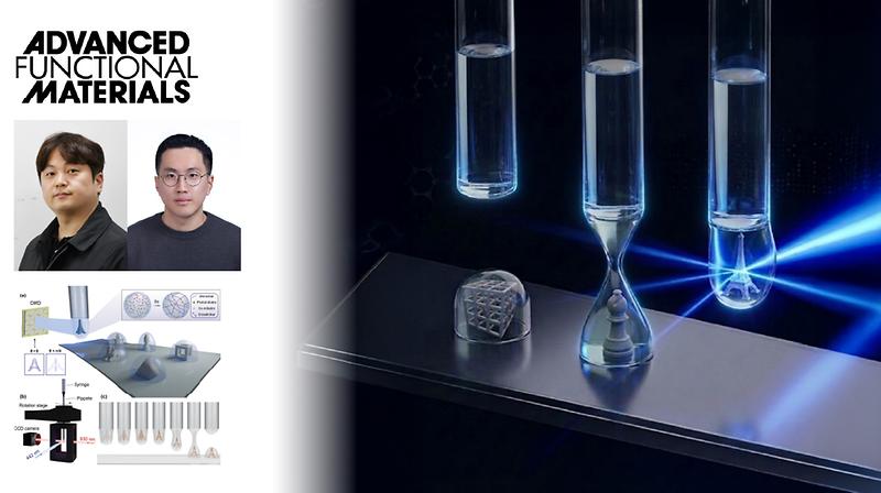
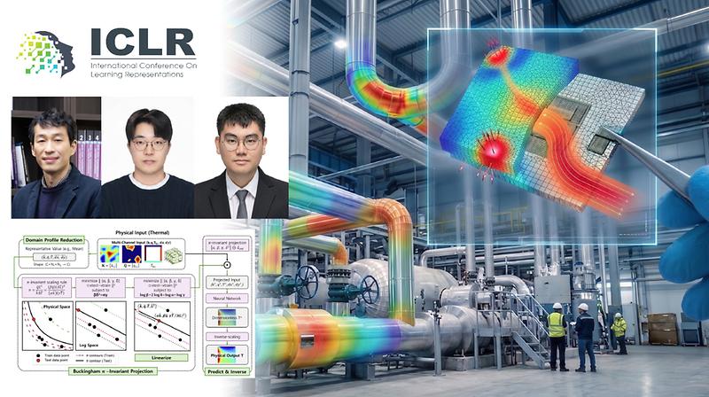
Abstract Despite the advantages of additive manufacturing (AM) in creating customized 3D shapes, conventional layer-by-layer approaches are limited by low production rates, restricting their broader applications. Volumetric additive manufacturing (VAM) has emerged as a promising technique, enabling the simultaneous photopolymerization of entire volumes, which significantly reduces fabrication time. However, current computed axial lithography requires manual operations per print cycle, such as loading resin into a vial, physically placing and aligning the vial (with or without an index-matching medium), and removing the printed object, limiting continuous, high-throughput production of multiple parts. Here, we propose a dispensing volumetric additive manufacturing (DVAM) method that prints and dispenses each part within a droplet in less than a minute. The printing process occurs within a single droplet dispensed from a glass pipette, enabling simultaneous printed object removal and resin replenishment in a second. Light pattern distortion caused by the absence of the index-matching fluid was corrected through real-time droplet profile estimation and inverse ray-tracing within the optical system. We demonstrate rapid serial VAM of 10 different objects within 10 min. This approach establishes a practical pathway toward scalable, high-throughput volumetric manufacturing, enabling rapid production of complex 3D structures without the operational bottlenecks of conventional VAM workflows. A research team affiliated with UNIST has achieved a major breakthrough in 3D microfabrication, enabling the rapid production of intricate 3D structures within a single minute. The new technology promises to significantly accelerate manufacturing processes in fields, ranging from biomedical devices to microelectronics. Led by Professor Im Doo Jung from the Department of Mechanical Engineering at UNIST, the research team developed a cutting-edge dispensing volumetric additive manufacturing (DVAM) system.The new approach moves beyond traditional layer-by-layer methods, allowing for the swift, continuous fabrication of diverse three-dimensional shapes within a matter of minutes by employing a volumetric printing process. DVAM utilizes a fine resin droplet dispensed from a glass pipette as the entire build volume. Light is projected onto the droplet to cure the desired shape in real-time. Once a structure is solidified, compressed air expels the finished object, and a new droplet is immediately dispensed for the next cycle. This seamless process enables high-speed, continuous production without the need for post-processing or layer-by-layer assembly. Unlike conventional volumetric printing methods—such as Computed Axial Lithography (CAL)—which require filling a resin container, matching refractive indices with immersion fluids, and manually removing finished parts, the UNIST team’s approach eliminates these constraints. By performing printing within a single resin droplet that acts as the entire volume, they achieve rapid, uninterrupted manufacturing. One of the main challenges was optical distortion caused by the droplet’s curved surface. To overcome this, the researchers integrated artificial intelligence with inverse ray-tracing optical calculations. A deep learning-based AI accurately detects the droplet’s profile in real-time, enabling the system to mathematically correct for distortions and project precise light patterns for uniform curing. This advanced system successfully produced intricate structures, such as the Eiffel Tower and The Thinker, within just 10 minutes—demonstrating the ability to fabricate ten different objects with an average time of around 60 seconds each. Hongryung Jeon, the first author of the study, explained, “Unlike traditional 3D printing that builds objects layer by layer, our method cures the entire volume at once and continuously dispenses resin without additional post-processing, increasing speed by over 100 times. This opens up exciting possibilities for large-scale, rapid production of micro-scale components.” Professor Jung, the corresponding author, emphasized, “Speed has long been a limiting factor in 3D printing, especially for customized manufacturing. By moving away from conventional photopolymerization and employing artificial intelligence to compensate for optical distortions, we have significantly advanced the potential of ultrafast volumetric fabrication. Now, complex shapes can be produced in seconds—eliminating long wait times.” The findings of this research have been published online in Advanced Functional Materials (Impact Factor: 19.0, top 5% in JCR) on March 21, 2026. The project was supported by the National Research Foundation of Korea (NRF), the Ministry of Science and ICT (MSIT), the Institute for Information & communications Technology Planning & Evaluation (IITP), and the Ministry of Trade, Industry & Energy (MOTIE). Journal Reference Hongryung Jeon, Yunsoo Lee, Seobin Park, et al., "Dispensing Volumetric Additive Manufacturing," Adv. Funct. Mater., (2026).

2026.05.12

  • 3D Printing
  • Advanced Functional Materials
  • CAL
  • Computed Axial Lithography
  • Department of Mechanical Engineering
  • DVAM
  • Im Doo Jung
  • Layer-by-Layer
  • Lithography
  • ME

New AI Algorithm to Enhance Accuracy of Thermal and Stress Predictions in Semiconductors

Abstract PDE surrogate models such as FNO and PINN struggle to predict solutions across inputs with diverse physical units and scales, limiting their out-of-distribution (OOD) generalization. We propose a π-invariant test-time projection that aligns test inputs with the training distribution by solving a log-space least squares problem that preserves Buckingham π-invariants. For PDEs with multidimensional spatial fields, we use geometric representative π-values to compute distances and project inputs, overcoming degeneracy and singular points that limit prior π methods. To accelerate projection, we cluster the training set into K clusters, reducing the complexity from O(MN) to O(KN) for the M training and N test samples. Across wide input scale ranges, tests on 2D thermal conduction and linear elasticity achieve MAE reduction of up to ≈91% with minimal overhead. This training-free, model-agnostic method is expected to apply to more diverse PDE-based simulations. A research team affiliated with UNIST has introduced a novel AI-based algorithm that enhances the accuracy of thermal and mechanical predictions across various scales, from microchips to large pipelines. Led by Professor Changwook Jeong from the Graduate School of Semiconductor Materials and Devices Engineering, their π-invariant test-time projection method realigns input data to conform with physical laws, addressing a crucial challenge in AI modeling—accurate predictions when faced with unfamiliar or out-of-distribution data. The algorithm identifies the most physically similar data within existing training sets based on a dimensionless ratio derived from Buckingham's π theorem. It then transforms new inputs into familiar, physically consistent forms without retraining the model, operating in log space to preserve physical ratios. This approach is computationally efficient, reducing processing costs by approximately 99% compared to traditional methods. Applied to 2D thermal conduction and linear elasticity problems, the technique achieved up to a 91% reduction in prediction error, even under conditions outside the original training range. It also demonstrated promising results in fluid dynamics, improving the accuracy of Navier–Stokes equation predictions in complex scenarios. This advancement is expected to accelerate and economize simulations in semiconductor design, packaging reliability, battery management, and structural safety analysis—fields where varying sizes and conditions demand both precision and efficiency. The study has been supported by the National Research Foundation of Korea (NRF) and the Institute of Information & Communications Technology Planning & Evaluation (IITP). Journal Reference Seokki Lee, Min-Chul Park, Giyong Hong, and Changwook Jeong, "Buckingham π-Invariant Test‑Time Projection for Robust PDE Surrogate Modeling," ICLR 2026 .

2026.05.11

  • AI Algorithm
  • Buckingham-pi
  • Changwook Jeong
  • Department of Materials Science and Engineering
  • ICLR
  • MSE
  • Navier–Stokes
  • PDE
  • SE
  • Semiconductor
  • Stress Predictions
  • Thermal Prediction

New Study Unveils Viral DNA ‘Barcode’ that Activates Innate Immunity, Opening New Therapeutic Avenues

Abstract Herpes simplex virus type 1 (HSV-1) infection remains a major global health challenge, yet the mechanisms underlying strain-specific innate immune responses are poorly understood. Here, we show that distinct HSV-1 strains differentially activate the absent in melanoma 2 (AIM2) inflammasome. The HF strain robustly induces AIM2-dependent inflammasome activation, whereas the F and KOS strains elicit minimal responses despite comparable infection efficiency. We demonstrate that this difference is driven by viral genomic features rather than replication capacity. Genomic analyses identify a poly(T) DNA sequence within the UL25-UL26 intergenic region that is enriched in the HF strain. Deletion of a 14-mer poly(T) sequence markedly impairs inflammasome activation, cytokine release, and host protection in vivo, whereas introduction of a poly(T) tract into the F strain is sufficient to confer AIM2 activation and enhanced host defense. Furthermore, poly(T)-mediated AIM2 activation is length-dependent, conserved in human macrophages, and requires a cGAS-STING-IRF1 licensing axis. Together, these findings identify viral poly(T) DNA as a key determinant of strain-specific AIM2 inflammasome activation and reveal how viral genomic variation shapes innate immune recognition. A research team, led by Professor SangJoon Lee from the Department of Biological Sciences at UNIST has identified a specific viral DNA sequence that triggers the body’s innate immune system, offering new insights into viral detection mechanisms and potential avenues for immunomodulatory therapies. In collaboration with Professor Joo Sang Lee from Sungkyunkwan University, Professor Eui Tae Kim from Jeju National University, and Director Young Ki Choi from the Korea Virus Research Institute at the Institute for Basic Science (IBS), the team demonstrated that a repetitive poly(T) sequence within the genome of herpes simplex virus type 1 (HSV-1) functions as a molecular barcode recognized by the innate immune sensor AIM2. HSV-1 infects about 67% of the global population and remains dormant in nerve cells, evading immune detection. Upon reactivation, it infects epithelial cells, provoking inflammation as part of the host’s defense. The study revealed that AIM2, a pivotal immune sensor in macrophages, detects the virus by recognizing poly(T) tracts—regions of repeated thymine (T) nucleotides—in its DNA. Importantly, immune activation was shown to depend on both the presence and length of this poly(T) sequence: longer repeats elicited stronger inflammatory responses and induced apoptosis in infected cells. Strains lacking the sequence or with fewer than 20 thymine bases elicited minimal immune activity. Introducing the poly(T) sequence into less responsive strains restored immune detection, with increased length correlating to heightened responses. These findings were confirmed in animal models, where viruses containing the poly(T) motif triggered inflammation and suppressed viral replication, while those without it led to unchecked proliferation and more severe disease outcomes. Further genomic analysis revealed that similar poly(T) repeats are conserved across various pathogenic viruses—including orthopoxviruses, adenoviruses, and coronaviruses—indicating a shared mechanism of immune recognition. “This study demonstrates that innate immune sensors recognize viral genomes with greater specificity than previously thought,” said Professor Lee. “Targeting these sensing pathways, rather than the viruses themselves, may offer innovative therapeutic options. Our research provides a foundation for developing immunomodulatory treatments for infectious diseases.” He added, “Given the conservation of this sequence across multiple viruses associated with severe illnesses, understanding its role could help link viral genomic features to disease severity and inform the design of targeted therapies.” Published in Nature Communications on April 13, the study was supported by multiple funding agencies, including the National Research Foundation of Korea (NRF), the Korea Health Industry Development Institute (KHIDI), the Ministry of Health and Welfare (MOHW), the Institute for Basic Science (IBS), the Circle Foundation, and Yuhan Corporation. Journal Reference SuHyeon Oh, Jueun Oh, Kyeongchan Im, et al., "Herpes simplex virus 1 harboring poly(T) DNA sequences as a key ligand for AIM2 inflammasome activation and host defense," Nat. Commun., (2026).

2026.05.04

  • Bio
  • Department of Biological Sciences
  • DNA
  • Herpes
  • Nature Communications
  • SangJoon Lee

Re‑Engineering the Future: For A More Resilience World

《 Editor's Note: Across fields that range from energy engineering to quantum physics, UNIST researchers share a common aim: redesigning the systems that sustain life and technology. Their latest work—converting solar‑panel waste into clean hydrogen, restoring vision through nanomedicine, and decoding the feedback loops driving global wildfires—positions science not merely as discovery, but as a blueprint for resilience.》 Sensing the Future From visions that steer robots to displays sharper than reality, UNIST researchers are redefining how machines interpret the human world. A smart contact lens equipped with AI‑driven sensors enables vision‑based robotic control, while a new quantum‑dot technique achieves over 4,000 pixels per inch—paving the way for ultra‑compact extended‑reality glasses. On a different frontier, three papers accepted to ICLR 2026 show the university's rising influence in reinforcement learning, advancing physical AI systems that learn directly from their environments. Together, these studies represent technology that doesn't just emulate perception—it extends it. • Smart Contact Lens for Vision-Based Robotic Control (Adv. Funct. Mater. l Mar., 2026) • Breakthrough QD Display with 4,000 PPI Resolution (Nat. Commun. l Mar., 2026) • Three Research Papers Accepted to ICLR 2026 Circulating Energy What if waste could power the next energy revolution? Two separate breakthroughs at UNIST bring that vision closer. One process converts end‑of‑life solar panels into high‑purity hydrogen and silica using mechanochemical reactions; Another turns industrial glycerol into hydrogen and value‑added chemicals through a scalable electrochemical system. Both replace extraction with regeneration, showing how circular design can meet industrial scale without environmental cost. This emerging “loop thinking” is central to UNIST's broader push toward a sustainable hydrogen economy. • Solar Panel Waste into H2 and High-Value Silica (Joule l Mar., 2026) • Turning Waste Glycerol into H2 and High-Value Chemicals (Joule l Mar., 2026) Healing Systems At the intersection of biology and environment, UNIST scientists are uncovering how systems heal themselves. A nanomedicine platform that selectively removes aging retinal cells restores vision in degenerative models, while another study reveals how alcohol and immune signaling interact to amplify liver damage—insights that could guide future therapies. On a planetary scale, researchers have identified a climate “regime shift” behind Australia's increasing wildfire intensity and developed AI frameworks for real‑time multilevel air‑pollution prediction. From cells to climate, the common thread is understanding how complex networks can recover balance. • Targeted Nanoparticles Aging Retinal Cells (Nat. Commun. l Mar., 2026) • Alcohol Amplifies Liver Damage During Illness (Sci. Adv. l Apr., 2026) • Climate Prediction (Nat. Commun. l Mar., 2026 ) • Wildfire Prediction (Agric. For. Meteorol. l Apr., 2026 ) • Deep Learning for Multiple Air Pollutant Analysis (Environ. Sci. Technol. l Mar., 2026) Across its laboratories, UNIST demonstrates that resilience is not a separate discipline—it is a design principle. By approaching technology, energy, and biology as interconnected systems, these efforts move beyond repair. They point instead toward a more fundamental question: How Can the World Be Designed to Endure—and Renew?

2026.05.01

  • Aging Retinal Cells
  • Alcohol
  • Climate Regime Shift
  • Hydrogen Economy
  • Liver Damage
  • Nanomedicine
  • Wildfires

Breakthrough QD Display Technology Achieves 4,000 PPI Resolution — Ideal for XR Glasses

Abstract Colloidal quantum dots (QDs) are leading candidates for next-generation optoelectronics owing to their tuneable bandgaps, narrow emission linewidths, and high luminescence quantum yields. For virtual-, augmented-, and mixed-reality display applications of these materials, patterning full-color QDs at μm-length scales is essential. However, existing photolithographic approaches often degrade QD luminance characteristics by exposing them to harsh processing conditions, or they compromise the structural fidelity of the resulting patterns. Here we report a photoresist-guided indirect (PIN) photopatterning strategy that includes (i) lithographic formation of sacrificial PR patterns, (ii) deposition of a crosslinked QD film on top, and (iii) PR stripping that removes the sacrificial PR, leaving behind crosslinked QD patterns on the substrate. QD crosslinking is mediated by a diazo-based ligand thermocrosslinker, Diazo-4-LiXer. Leveraging low-temperature (110–120 °C)-activated carbene chemistry, Diazo-4-LiXer bridges neighbouring QDs while maintaining their intrinsic photoluminescence and electroluminescence through repeated processing. Moreover, Diazo-4-LiXer enables thermocrosslinking without affecting the underlying photoresist pre-patterns, which serve as structural templates determining the thickness and fidelity of the QD patterns. Using PIN photopatterning, we realize high-fidelity RGB patterns exceeding 4,000 pixels per inch resolution and demonstrate integration-level scalability by fabricating a 10 × 10 passive-matrix full-colour RGB QD–LED array. Researchers, affiliated with UNIST have announced a significant advancement in quantum dot (QD) display technology, enabling ultra-fine, high-resolution patterning of QDs suitable for next-generation XR glasses. This innovation promises brighter, more vivid images even in outdoor environments. Professor BongSoo Kim from the Department of Chemistry at UNIST, in collaboration with Professor Moon Sung Kang of Sogang University and Dr. Chan-mo Kang at Electronics and Telecommunications Research Institute (ETRI), have developed a novel photopatterning technique that maintains the integrity of quantum dots while achieving micron-scale precision. To meet the demanding resolution required for XR displays—exceeding 3,000 pixels per inch (PPI)—the team’s method patterns quantum dots into 2-micrometer (μm) pixels. This enables over 4,000 PPI, meaning more than 10 million pixels can be packed into a space about the size of a coin, ensuring sharp, immersive visuals. The process employs a custom-developed additive, Diazo-4-LiXer, which facilitates thermocrosslinking at low temperatures (110–120°C) via carbene chemistry, preserving the quantum dots’ luminescent properties. It involves creating a sacrificial photoresist (PR) template, depositing a crosslinked quantum dot film, then removing the PR to leave behind precisely patterned quantum dots—without damage or shape distortion. This technique not only achieves high fidelity and density but also enables the fabrication of full-color RGB quantum dot LED arrays, demonstrating its potential for commercial application. Professor Kim commented, “Our method allows for ultra-high resolution patterning of quantum dots while maintaining their exceptional optical properties. It opens new avenues for advanced XR glasses and microdisplays, where brightness, color purity, and resolution are crucial.” The findings of this research have been published in Nature Communications on March 19, 2026. The study has been supported by the Samsung Research Funding & Incubation Center of Samsung Electronics, the National Research Foundation of Korea (NRF), and the Ministry of Science and ICT (MSIT). Journal Reference Hyeokjun Kim, Hyobin Ham, Chang Hyeok Lim, et al., "Photoresist-guided indirect photopatterning of quantum dots via carbene-mediated ligand thermocrosslinking," Nat. Commun., (2026).

2026.04.27

  • 4000PPI
  • BongSoo Kim
  • Chemistry
  • Crosslinker
  • Department of Chemistry
  • Microdisplay
  • Nature Communications
  • Pattern Fidelity
  • Photopatterning
  • Photoreist
  • QD-LED
  • Quantum Dot
  • Thermocrosslinking
  • VR
  • XR

더보기

UNIST Insight

star

UNISTAR Voices 
Shaping Futures, 
Inspiring the 
World

더보기

Life at UNIST

star